The hardware architecture post of this series covered the three hardware variants per the SWS. This post goes one level deeper: what happens at the PCB level when a frame travels from the host, through the switch, to an external port?
The host-side interfaces
The host SoC connects to the switch chip via the same MAC-side interfaces
used in a plain EthTrcv setup — the electrical interface doesn’t
distinguish between "talking to a single PHY" and "talking to a switch".
With higher port counts and bandwidth, RGMII or SGMII is typically used:
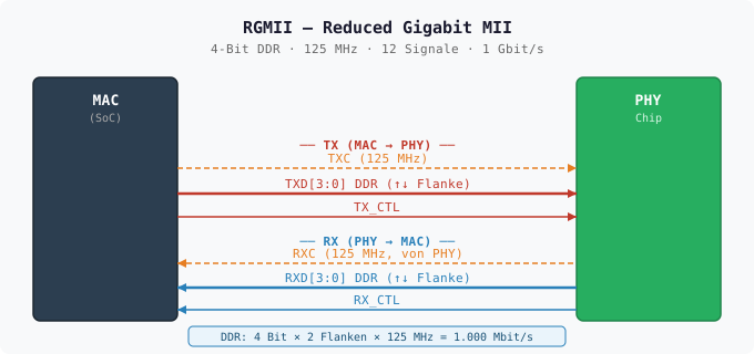
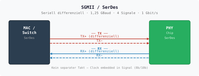
Both diagrams come from this blog’s EthTrcv hardware deep dive — the electrical specification of RGMII/SGMII doesn’t change just because a switch sits on the other end instead of a single PHY. For a switch, read "PHY" in the diagrams as "switch" accordingly. |
Internal port-to-port connections
The key difference from a plain transceiver setup: there’s no classic bus between the external ports that the host could tap into. The forwarding decision happens entirely inside the switch, as shown below:
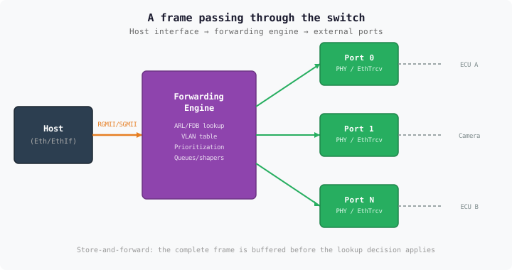
In this architecture, the host only sees frames addressed to itself, plus whatever it explicitly requests via mirroring (see Part 4 of this series).
Embedded vs. external PHYs
As shown in the hardware architecture post, the physical connection of the external ports depends on the hardware variant:
Embedded PHYs (variant 2) — no extra IC per port, the switch chip itself drives the line
External PHYs (variants 1 and 3) — a standalone
EthTrcvchip per port, connected via MII/MDIO
For the MDI (Medium Dependent Interface) — i.e. the actual cable connection — the same considerations apply as for a plain transceiver: single-pair cabling for 100BASE-T1/1000BASE-T1, automotive connectors (FAKRA, HSD, MATEnet), EMC filtering via common-mode chokes.
Power sequencing on multi-port chips
A switch chip with multiple (possibly embedded) PHYs has a considerably
more complex power-sequencing problem than a single PHY: several voltage
rails (core, I/O, per-port PHY analog section) have to come up in the
correct order before EthSwt_Init can even successfully access the
registers (see ETHSWT_E_ACCESS in Part 2 of this series). In the worst
case, a single mis-sequenced port can block the entire switch boot if the
chip waits on reset for a shared internal bus fed by all domains.
EMC aspects of densely packed ports
Several high-frequency lines (RGMII at 125 MHz DDR, multiple single-pair cables) packed closely together on a board increase the risk of crosstalk between neighboring ports. In practice that means: adequate trace spacing, consistent ground planes between port groups, and careful routing matter even more for multi-port switches than for a single PHY.
From bit to signal — a frame through the switch
The frame arrives at the host interface (RGMII/SGMII)
The forwarding engine performs the ARL/FDB lookup (see the ARL table post)
VLAN and priority handling per the ingress configuration (Parts 3/4)
Enqueuing into the appropriate egress queue (see the TSN post on shapers)
Output at the destination port, possibly with VLAN retagging
Switches generally operate in store-and-forward mode: a frame is buffered completely before the forwarding decision is made — as opposed to cut-through, where forwarding starts right after the header. That costs extra latency (proportional to frame size), but is necessary to check the CRC before forwarding, so a corrupted frame doesn’t get spread across the whole network. |
Summary
| Aspect | Key takeaway |
|---|---|
Host interface | RGMII/SGMII — the same electrical specification as a plain EthTrcv setup |
Internal frame path | Runs entirely inside the switch via the forwarding engine; the host only sees relevant or mirrored frames |
Power sequencing | Considerably more complex on multi-port chips than on a single PHY |
Store-and-forward | The default for automotive switches — costs latency but ensures CRC checking before forwarding |